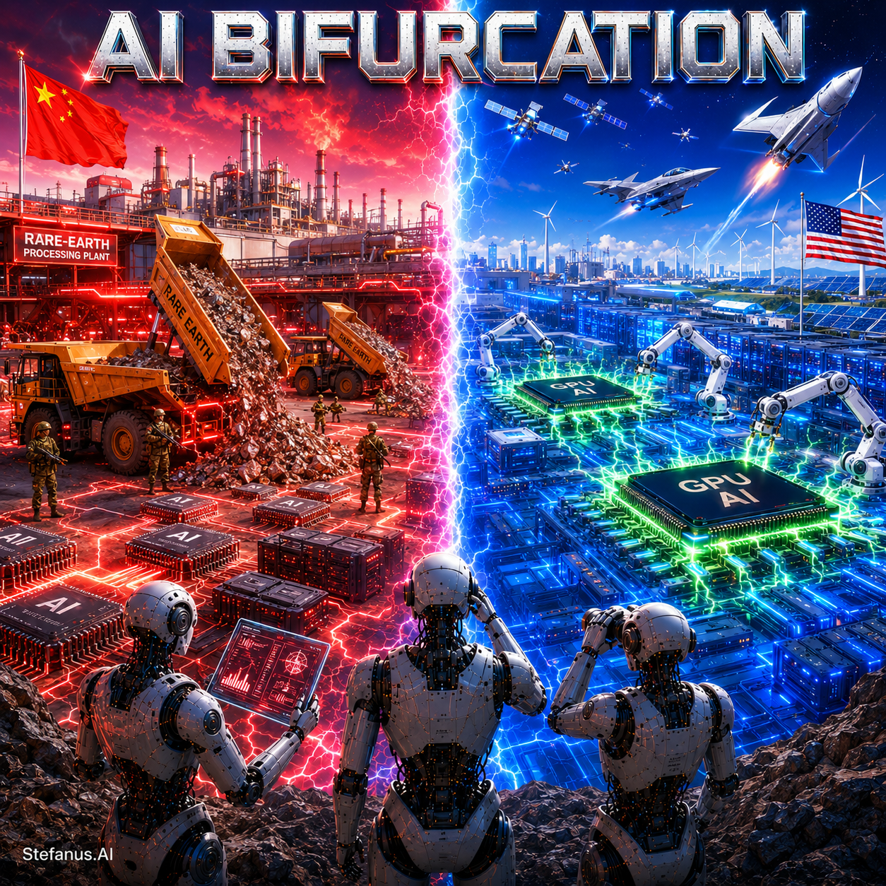
Introduction: From “Drill, Baby, Drill” to “Chip, Baby, Chip”
Every industrial age eventually produces its own slogan. The oil age produced the language of extraction, the factory age produced the language of production, the internet age produced the language of scale, and the artificial intelligence age is now producing the language of compute. In the 2024 United States presidential campaign cycle, one of the most recognizable political slogans to return to public life was the old energy phrase “drill, baby, drill,” a phrase built around the idea that national power could be expanded by accelerating domestic production of oil and gas. It was simple, aggressive, and memorable. It implied that the answer to national vulnerability was not restraint, but production; not dependence, but extraction; not waiting, but building. In the artificial intelligence era, that same industrial instinct is being rewritten in semiconductor form. The new doctrine is not merely “drill, baby, drill.” It is “Chip, Baby, Chip.”
This paper uses “Chip, Baby, Chip” as a metaphor for the rapid, sometimes chaotic, and increasingly geopolitical race to manufacture the hardware foundation of artificial intelligence. The phrase is intentionally provocative because the moment itself is provocative. The word “chip” here has nothing to do with potato chips, snack food, or consumer branding. It refers to the microprocessor, the accelerator, the GPU, the TPU, the inference engine, the high-bandwidth-memory stack, and the increasingly specialized silicon architecture that allows modern AI systems to train, reason, infer, recommend, classify, generate, simulate, and act. If oil was the combustible input of the twentieth-century industrial economy, chips are the computational input of the twenty-first-century intelligence economy.
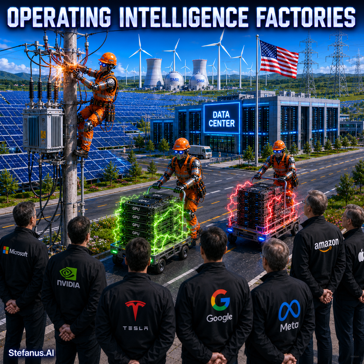
In Jensen Huang’s five-layer AI economy, energy sits at the first layer and chips sit immediately after it. That order matters. Energy is the physical base, but chips are the conversion mechanism through which electricity becomes computation, computation becomes models, models become applications, and applications become agentic systems. The AI economy therefore does not begin in the software interface. It begins in power plants, substations, fabs, lithography machines, advanced packaging lines, memory supply chains, and hyperscale data centers. The visible chatbot is only the surface of the system. Beneath it is an industrial stack.
Vaclav Smil’s famous observation about energy captures the deeper structure of this transformation:
“Energy is the only universal currency.”¹
In the AI era, chips are becoming the exchange mechanism of that currency. Energy alone cannot produce intelligence. A power plant without accelerators is only a power plant. But when electricity moves through GPUs, TPUs, ASICs, memory stacks, and interconnect fabrics, it becomes artificial cognition. That conversion is why semiconductors have become the most important industrial object in the world. They sit at the intersection of economics, defense, infrastructure, science, and state power.
This is why the race has become so intense. Hyperscale companies are no longer content to buy chips passively from the market. They are designing their own silicon, reserving foundry capacity years in advance, building proprietary inference systems, funding power infrastructure, partnering with governments, and trying to reduce dependence on a small number of suppliers. NVIDIA still dominates the AI accelerator market through its GPUs and CUDA software ecosystem. TSMC remains the dominant advanced foundry. ASML remains the indispensable lithography supplier for extreme ultraviolet systems. Google is pushing TPUs deeper into the agentic AI era. Amazon Web Services is expanding Trainium, Inferentia, and Graviton. Meta is accelerating its MTIA roadmap. Intel is attempting to reenter the advanced foundry race through 18A and 14A. Elon Musk’s Terafab vision, now tied to Tesla, SpaceX, and Intel, represents perhaps the most extreme version of vertical integration: one industrial compute system for cars, robots, AI data centers, and eventually space-based infrastructure.²
The urgency is not imaginary. The International Energy Agency reported that global electricity demand from data centers grew by 17% in 2025, while electricity consumption from AI-focused data centers surged by 50%.³ The same IEA analysis projects that data-center electricity consumption could roughly double by 2030 to about 945 terawatt-hours, representing just under 3% of global electricity consumption.⁴ This means that the AI chip race is not only a semiconductor race. It is also a grid race, an energy race, a cooling race, a land race, a permitting race, a memory race, and a geopolitical race.
The IEA’s framing is blunt:
“Electricity consumption from AI-focused data centres grew even faster, surging 50% in 2025.”³
That single sentence explains the new industrial anxiety. If the software layer continues to scale, the hardware layer must scale. If models require more training, more inference, more agentic reasoning, more memory, and more multimodal processing, then chips must multiply. If chips multiply, fabs must expand. If fabs expand, power demand rises. If power demand rises, the grid becomes a strategic battlefield. This is the logic of “Chip, Baby, Chip.”
Yet the slogan also carries a warning. “Drill, baby, drill” implied that more extraction would solve the energy problem, but the real world proved more complicated. Extraction created abundance, but also environmental cost, geopolitical dependency, and infrastructure stress. “Chip, Baby, Chip” faces the same danger. More chips can accelerate AI, but more chips alone cannot guarantee resilience. A nation can manufacture more accelerators and still remain dependent on foreign lithography tools, rare-earth processing, high-bandwidth memory, advanced substrates, and offshore assembly. A hyperscaler can buy millions of GPUs and still face power bottlenecks. A government can pass a semiconductor subsidy bill and still struggle with skilled labor, water use, environmental review, and state-level permitting.
Therefore, this paper does not treat “Chip, Baby, Chip” as a blind celebration of semiconductor expansion. It treats it as a doctrine of urgency that must mature into a doctrine of sovereignty, efficiency, and infrastructure discipline. The United States must build more chip capacity, but it must also build smarter chip capacity. It must reshore more manufacturing, but also secure the materials, machines, talent, and energy that make manufacturing possible. It must accelerate AI hardware, but not create an energy-waste civilization where brute-force compute becomes the only answer to every model problem.
Chris Miller, author of Chip War, has argued that semiconductors are now central to economic and geopolitical power:
“No product is more central to international trade than semiconductors.”⁵
That is the world “Chip, Baby, Chip” enters. It is a world where AI companies compete not only over models, but over wafers. It is a world where national security is measured not only by aircraft carriers and missiles, but by EUV machines, HBM supply, packaging capacity, and export controls. It is a world where the future of intelligence may be decided by who controls the physical machinery of computation.
Section 1: Why “Chip, Baby, Chip?” and the Rise of AI Hardware
The rise of AI hardware cannot be understood as a normal product cycle. It is not simply another wave of faster chips replacing slower chips. It is the beginning of a new industrial order in which the demand for computation is expanding faster than traditional semiconductor planning, grid planning, data-center planning, and national industrial policy were designed to handle. For decades, the digital economy depended on Moore’s Law, cloud computing, mobile devices, and software abstraction. Most users never had to think about the physical machinery behind computation. AI has ended that illusion. The intelligence economy has made hardware visible again.
Large language models, multimodal systems, diffusion models, robotics models, recommender systems, and agentic AI platforms have one thing in common: they consume enormous amounts of compute. Training a frontier model requires massive parallel processing, high-bandwidth memory, specialized networking, and clusters that can operate as a single machine. Inference requires an even more persistent layer of compute because every user query, every generated image, every recommendation, every code completion, every autonomous decision, and every agentic workflow triggers a new demand for silicon.
The AI industry first treated training as the main bottleneck. That made sense when the frontier race focused on building larger models. But the next economic bottleneck may be inference. Training is episodic; inference is continuous. Training builds the model; inference monetizes the model. Training consumes massive bursts of compute; inference consumes distributed, repeated, real-time compute across billions of interactions. This is why hyperscalers are investing so heavily in custom inference chips. The companies that control inference hardware will not simply reduce cost. They will control the decision layer of the AI economy.
“Chip, Baby, Chip” is therefore the hardware expression of AI acceleration. It captures the pressure to buy GPUs faster, build fabs faster, deploy data centers faster, patent custom silicon faster, and reduce dependence on foreign manufacturing faster. It is a slogan of speed, but it is also a slogan of fear: fear that the United States may not have enough domestic chip capacity; fear that China may gain compute independence; fear that a Taiwan Strait crisis could paralyze advanced AI development; fear that NVIDIA’s dominance could become a single-vendor bottleneck; fear that energy grids cannot support the next decade of AI growth.
The urgency is visible in energy projections. The IEA’s 2026 analysis describes data centers as the “critical infrastructure for training and running AI models,” and projects that data-center electricity use could reach around 945 TWh by 2030.⁴ That figure is not a footnote to the AI story. It is the physical price of intelligence. Every AI chip is an energy-consumption device. Every GPU rack is a demand signal to the grid. Every hyperscale training cluster is a claim on electricity, water, cooling, land, and transmission.
The IEA warns:
“Data centre electricity consumption grows by around 15% per year.”⁴
That growth rate places AI infrastructure outside the comfort zone of ordinary utility planning. Power grids were not designed around sudden multi-gigawatt digital-industrial campuses. Semiconductor fabs were not designed to be built overnight. Transmission lines are not approved at software speed. Nuclear plants are not deployed on venture-capital timelines. The result is a mismatch between the velocity of AI ambition and the slower tempo of physical infrastructure.
This is why chips have become the new “oil” of the AI economy. But the analogy must be handled carefully. Oil is extracted from geology; chips are manufactured through one of the most complex industrial processes humanity has ever created. Oil supply depends on reserves, drilling, refining, pipelines, and shipping. Chip supply depends on design tools, wafers, photoresists, gases, EUV machines, clean rooms, high-purity chemicals, metrology, packaging, memory, substrates, and ultra-specialized engineering labor. Oil shaped the twentieth-century geopolitics of the Middle East, Russia, and the United States. Chips now shape the geopolitics of Taiwan, the Netherlands, Japan, South Korea, China, and the United States.
The central strategic problem is that the AI chip supply chain is both global and concentrated. TSMC manufactures a large share of the world’s most advanced chips. ASML supplies the EUV lithography systems required for cutting-edge nodes. South Korean firms dominate high-bandwidth memory. China controls important portions of rare-earth processing and critical minerals. The United States leads in many chip-design companies and EDA tools, but it no longer dominates fabrication the way it once did. This is the architecture of dependency.
In this sense, “Chip, Baby, Chip” is not only a corporate race. It is a national reindustrialization argument. The United States wants to bring back semiconductor manufacturing not because every chip must be made domestically, but because no serious AI superpower can rely entirely on fragile foreign chokepoints for the computational base of its economy and defense system. The CHIPS and Science Act reflects this strategic recognition. The Commerce Department says CHIPS for America has allocated over $32 billion in proposed funding across 16 states to support domestic factories and semiconductor programs.⁶
The question, however, is whether subsidy alone can overcome the deeper physics of the semiconductor stack. Fabs require enormous capital, stable policy, skilled labor, water, and power. They require clusters of suppliers. They require long learning curves. They require yield improvement. They require trust from customers who will not risk advanced designs on unproven foundry processes. Industrial sovereignty is not declared; it is manufactured over years.
This is why the phrase “Chip, Baby, Chip” must be understood as both call and caution. The call is clear: build more. The caution is equally clear: build intelligently. The AI era cannot survive on hardware maximalism alone. It needs performance-per-watt, co-design, advanced packaging, domestic capacity, resilient supply chains, and energy-aware computing. Otherwise, the United States may win the race to deploy chips while losing the larger race to build sustainable compute civilization.
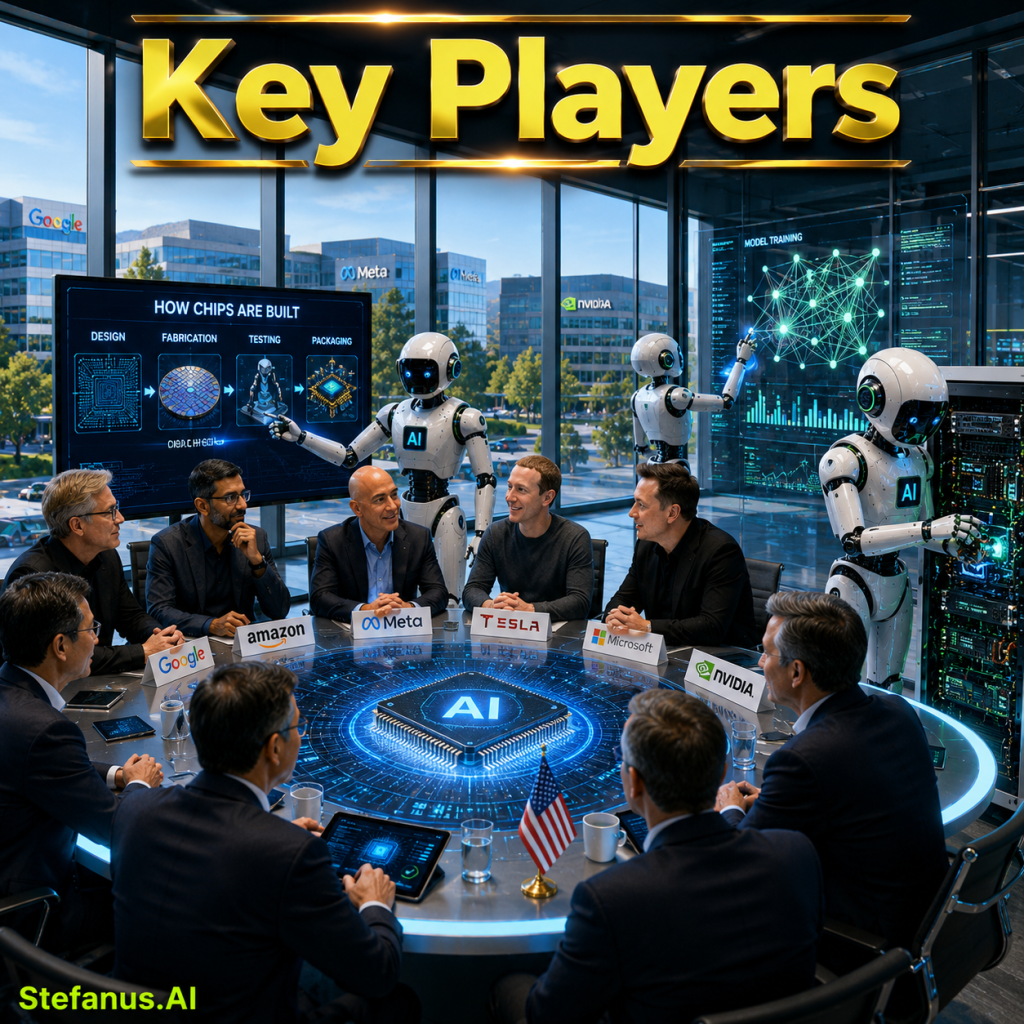
Section 2: Key Players and Strategies in the AI Chip Race
The AI chip race is not a single contest between one company and another. It is a layered industrial struggle in which different companies occupy different strategic positions in the compute stack. NVIDIA dominates accelerators and software ecosystems. TSMC dominates advanced fabrication. ASML dominates EUV lithography. Intel is trying to rebuild American foundry credibility. Google, Amazon, Meta, Microsoft, Apple, Tesla, SpaceX, and other hyperscalers are building custom chips to reduce dependency, lower cost, improve efficiency, and gain control over the internal economics of AI. Each player is not merely selling products. Each is building a theory of the future.
The old semiconductor economy was organized around specialized roles: design firms designed chips, foundries manufactured them, cloud providers deployed servers, and software firms wrote applications. The AI economy is collapsing those boundaries. Hyperscalers now want to design chips. Chip companies now want to sell full data-center systems. Foundries now compete through packaging and geographic resilience. Governments now act like strategic investors. Energy companies now become AI infrastructure partners. The result is a new industrial map.
2.1 NVIDIA: The Empire of Accelerated Compute
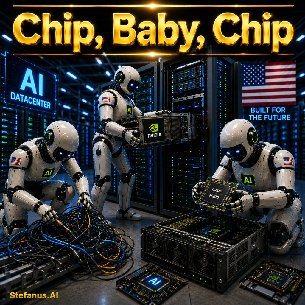
NVIDIA is the most visible symbol of the AI hardware revolution because it transformed the GPU from a graphics product into the central engine of machine learning. Its advantage is not only that its chips are fast. Its advantage is that its chips are embedded inside an ecosystem. CUDA, libraries, developer tools, networking systems, model frameworks, enterprise software, and hardware roadmaps all reinforce one another. Once AI labs optimize around NVIDIA, switching becomes expensive, risky, and slow.
Reuters reported in March 2026 that Blackwell chips were available for purchase and that Rubin chips were NVIDIA’s next-generation processors in full production.⁷ The same Reuters reporting described Blackwell and Rubin as flagship AI chips capable of building the large language models underlying systems like ChatGPT.⁷ That point matters because NVIDIA is no longer merely selling cards into servers. It is selling the infrastructure of model civilization.
NVIDIA’s strategy is to move from chips to systems. The company increasingly thinks in rack-scale architectures, high-speed interconnects, networking fabrics, CPUs, GPUs, software stacks, and total data-center performance. The GPU is no longer isolated. It is part of a machine that must behave like a single intelligence factory. This is why Blackwell, Grace Blackwell, Vera Rubin, NVLink, InfiniBand, Spectrum-X, and related systems should be understood as pieces of a unified compute empire.
The company’s dominance is also geopolitical. At the Milken Institute Global Conference in Los Angeles in May 2026, Jensen Huang reportedly argued that China should not have access to the most advanced Blackwell and Rubin AI GPUs and said the United States should have “the first, the most, and the best” in AI hardware.⁸
“The first, the most, and the best.”⁸
That quote is short, but it captures the new doctrine of compute nationalism. The leading AI chips are not treated like ordinary commercial products. They are treated like strategic assets. Export controls, licensing rules, China-specific chip variants, and domestic manufacturing debates all flow from the recognition that advanced compute is now dual-use infrastructure. It can power consumer chatbots, but it can also power cyber operations, military planning, weapons design, autonomous systems, intelligence analysis, and scientific discovery.
NVIDIA’s vulnerability is that its dominance depends on supply partners. Its flagship chips are manufactured by TSMC. Its systems depend on high-bandwidth memory supply, advanced packaging capacity, substrates, and power infrastructure. In other words, even the most powerful AI chip company in the world does not control the entire stack. This is why NVIDIA’s rise does not eliminate supply-chain fragility; it concentrates market power at one layer while leaving the deeper manufacturing stack distributed across Taiwan, South Korea, the Netherlands, Japan, and the United States.
2.2 TSMC: The Foundry Backbone of the AI Age
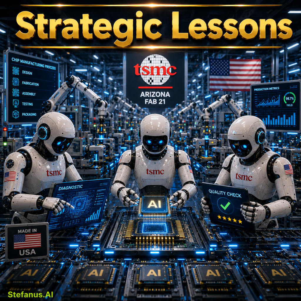
If NVIDIA is the empire of accelerated compute, TSMC is the industrial backbone behind much of that empire. TSMC’s foundry model allowed the world’s leading chip designers to outsource manufacturing while focusing on architecture, software, and product strategy. That model became one of the most successful industrial arrangements in modern history. In the AI age, however, TSMC has become more than a supplier. It has become a strategic chokepoint.
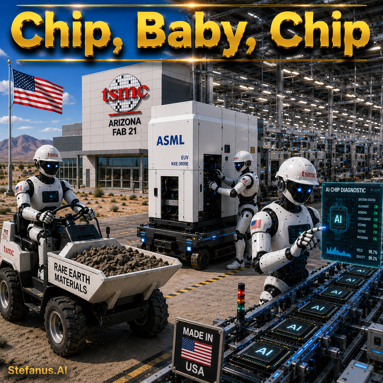
Reuters reported that TSMC is investing $165 billion in Arizona chip factories, while also planning a chip-packaging plant in Arizona by 2029.⁹ ¹⁰ This investment is not simply an expansion project. It is a symbol of the American attempt to rebuild advanced semiconductor capacity on U.S. soil. Arizona is becoming a test case for whether the United States can host a full advanced semiconductor ecosystem, not merely isolated fabs.
TSMC’s strategic position is strengthened by two realities. First, advanced-node manufacturing is brutally difficult. Yield, process control, contamination management, precision tooling, and production discipline separate true leading-edge fabs from aspirational announcements. Second, AI chips increasingly require advanced packaging, not merely transistor scaling. Reuters reported in April 2026 that TSMC aims to open an Arizona chip-packaging plant by 2029.¹⁰ Packaging matters because modern AI systems increasingly use chiplets, HBM stacks, interposers, and multi-die architectures. The future of AI compute may be decided as much by how chips are connected as by how small their transistors are.
This shift changes the meaning of manufacturing sovereignty. A country does not possess semiconductor sovereignty simply because it can fabricate wafers. It also needs packaging, memory integration, testing, substrates, chemicals, gases, and supply-chain redundancy. The chip is not one object. It is an ecosystem compressed into silicon.
TSMC’s Arizona expansion therefore represents progress, but also exposes the scale of the challenge. The United States can attract investment, but it must also create a durable industrial environment. That means skilled technicians, engineering education, permitting predictability, water infrastructure, reliable electricity, and supplier localization. Fabs are not apps. They cannot be spun up by ambition alone.
2.3 ASML: The Machine Behind the Machine
No discussion of AI chip manufacturing can ignore ASML. The Dutch company’s EUV lithography systems are among the most complex machines ever built, and they are indispensable for producing the most advanced chips. ASML explains that its NXE EUV systems use a 13.5 nm EUV light source and are used to print foundation layers for 7 nm, 5 nm, and 3 nm nodes.¹¹ Georgetown CSET describes ASML as the sole supplier of EUV machines.¹²
“ASML has emerged as the sole supplier of EUV machines.”¹²
This makes ASML a geopolitical hinge. The United States can design advanced chips. Taiwan can manufacture them. South Korea can supply memory. But without EUV lithography, the most advanced nodes become impossible to scale economically. ASML is therefore not merely a European industrial success story. It is a control point in the global AI economy.
Reuters reported in February 2026 that ASML unveiled an EUV light-source advance that could yield 50% more chips by 2030.¹³ That kind of improvement matters because EUV throughput affects fab economics. If exposure times fall and output rises, advanced chip capacity can expand without requiring a proportional increase in machines. But the broader point remains: the AI race depends on machines so rare, expensive, and complex that even major powers cannot easily replicate them.
ASML’s position also gives Europe a unique form of semiconductor leverage. The European Union may not dominate hyperscale cloud or AI model development in the same way as the United States and China, but Europe controls a crucial machine layer. This is why the EU’s regulatory power and ASML’s industrial power must be considered together. Europe may regulate AI through law, but it also shapes AI through lithography.
2.4 Intel and Terafab: The Return of American Foundry Ambition
Intel’s story is one of both decline and attempted resurrection. Once the symbol of American semiconductor supremacy, Intel lost ground to TSMC in advanced manufacturing and to NVIDIA in AI acceleration. But the AI era has created an opportunity for Intel to become strategically relevant again, not necessarily as the dominant chip designer, but as a domestic foundry platform.
Intel Foundry has emphasized process technologies such as 18A and 14A, including new specialized nodes and advanced system assembly and test capabilities.¹⁴ The company presents itself as a “systems foundry” for the AI era.¹⁵ This language is important because it suggests that foundry competition is no longer only about the smallest transistor. It is about packaging, assembly, supply-chain resilience, design enablement, and full-stack manufacturing services.
The most dramatic development is Elon Musk’s Terafab concept. Reuters reported in May 2026 that SpaceX filed plans for a $55 billion Terafab chip facility in Texas, with a possible expansion to $119 billion.¹⁶ Reuters also reported that Tesla plans to use Intel’s 14A manufacturing process for the Terafab project, potentially marking a major external customer win for Intel’s advanced foundry ambitions.¹⁷
The Terafab concept is important because it represents extreme vertical integration. Musk’s companies do not merely need chips for one product. Tesla needs chips for autonomous vehicles, robotaxis, and Optimus humanoid robots. xAI needs AI training and inference capacity. SpaceX may need chips for satellites, ground systems, and future space-based data centers. If all of those systems converge, then chip supply becomes a civilization-scale bottleneck inside one corporate ecosystem.
Reuters summarized the ambition as chips for Tesla self-driving systems, AI data centers, and humanoid robots.¹⁶ This is not ordinary corporate diversification. It is the attempt to build a unified compute-industrial platform across terrestrial mobility, robotics, AI, and space infrastructure. Whether Terafab succeeds or not, it reveals the direction of elite technology strategy: companies no longer want to wait for the market to allocate compute. They want to own the machines that produce the compute.
The risk is obvious. Semiconductor manufacturing is brutally capital-intensive and technically unforgiving. Musk’s timelines are often aggressive. Building a fab is not like launching a software product or scaling a social platform. It requires process maturity, tool procurement, clean-room execution, supplier coordination, and yield discipline. Reuters noted that many details remain unclear, including financing, operation, and timeline.¹⁸ But the concept itself matters because it shows how AI hardware has become so strategically central that even companies outside traditional semiconductor manufacturing now want to enter the fab race.
2.5 Google: TPU, Ironwood, and the Co-Designed AI Stack
Google has been building custom AI silicon for years, and its TPU strategy is one of the clearest examples of vertical integration in the AI era. Unlike NVIDIA’s general-purpose GPU approach, Google’s Tensor Processing Units are application-specific accelerators optimized for machine-learning workloads. The strategic logic is straightforward: if Google controls the model, the software framework, the cloud environment, the data-center architecture, and the chip, it can optimize across the entire system.
Google’s official Cloud blog describes Ironwood as its most powerful, capable, and energy-efficient TPU, designed for “thinking, inferential AI models at scale.”¹⁹
“Ironwood is our most powerful, capable and energy efficient TPU yet.”¹⁹
Google later announced its eighth generation of TPUs, TPU 8t and TPU 8i, describing them as chips built for training massive AI models and running complex AI agents.²⁰ This distinction between training and inference is crucial. The AI industry is maturing from one big-chip category into specialized compute classes. Training chips must maximize throughput and memory movement across enormous models. Inference chips must optimize latency, cost, reliability, and power efficiency at scale. Agentic AI adds another layer because reasoning systems may require persistent compute across multi-step tasks.
Google’s co-design advantage is not limited to the chip. Its Ironwood stack includes JAX, PyTorch support, XLA compiler integration, and high-level frameworks woven into the TPU platform.²¹ This is the deeper meaning of custom silicon: the chip is not merely hardware; it is part of a software-hardware organism. The more the stack is integrated, the more efficiency can be extracted from each watt.
This is why Google’s TPU strategy directly challenges the “buy more GPUs” model. If NVIDIA represents horizontal dominance through a widely adopted accelerator platform, Google represents vertical efficiency through internal control. Google does not need to sell TPUs in the same way NVIDIA sells GPUs. It can use TPUs to strengthen Google Cloud, Gemini, Search, YouTube, Workspace, and internal AI systems. The chip becomes a strategic internal advantage.
2.6 Amazon Web Services: Trainium, Inferentia, Graviton, and Cloud Economics
Amazon’s custom silicon strategy is different from Google’s, but equally important. AWS began designing chips after acquiring Annapurna Labs in 2015, focusing on chips optimized for cloud workloads, better performance, lower cost, and lower energy use.²² Its main chip families include Graviton CPUs, Inferentia inference accelerators, and Trainium training accelerators.
AWS describes Inferentia chips as designed to deliver high performance at the lowest cost in Amazon EC2 for deep learning and generative AI inference.²³ AWS describes Trainium2-based EC2 Trn2 instances and Trn2 UltraServers as purpose-built for generative AI, offering 30–40% better price performance than comparable GPU-based instances.²⁴
The economic logic is powerful. AWS operates at such scale that even modest improvements in performance-per-dollar and performance-per-watt can translate into enormous savings. Custom silicon allows AWS to reduce dependence on external suppliers, offer differentiated cloud services, and shape AI infrastructure economics for customers.
Amazon’s strategy also reflects the rise of inference as the commercial center of gravity. Training attracts attention because it produces frontier models, but inference produces recurring revenue. If millions of companies build AI applications on AWS, then the cost of serving those applications becomes a strategic variable. Inferentia exists because AI inference cannot remain permanently dependent on expensive general-purpose accelerators.
AWS’s chip strategy also strengthens its position as an infrastructure company. Amazon does not need to win the public narrative of model supremacy in the same way as OpenAI, Google DeepMind, or Anthropic. It can win by becoming the compute substrate on which others train and run models. In that world, Trainium and Inferentia are not side projects. They are AWS’s attempt to own the cost curve of AI.
2.7 Meta: MTIA and the Economics of Social-Scale AI
Meta’s AI hardware strategy is driven by one of the largest inference surfaces in the world: Facebook, Instagram, WhatsApp, Threads, advertising systems, ranking models, recommendation engines, and generative AI experiences across billions of users. Meta does not merely need chips for frontier model research. It needs chips for social-scale inference and recommendation workloads.
Meta announced in March 2026 that it is advancing four new generations of MTIA chips: MTIA 300, 400, 450, and 500.²⁵ Meta said MTIA 300 is already in production for ranking and recommendations training, while MTIA 400, 450, and 500 will support broader workloads and primarily GenAI inference production into 2027.²⁶ Reuters likewise reported that MTIA 300 is in use for ranking and recommendation systems and that later chips will roll out through 2027, with MTIA 450 and 500 designed for inference.²⁷
Meta’s roadmap reveals two important truths. First, AI chips are becoming workload-specific. A chip built for recommendation ranking is not necessarily the same as a chip built for frontier LLM training. Second, hyperscalers do not see custom silicon as optional. They see it as necessary for margin control, latency control, and strategic independence.
Meta is also simultaneously buying NVIDIA chips while developing its own. Reuters reported in February 2026 that NVIDIA announced a multiyear agreement to sell Meta millions of current and next-generation AI chips, including Blackwell and Rubin.²⁸ That dual strategy is important. Hyperscalers are not abandoning NVIDIA overnight. They are hedging. They buy NVIDIA for frontier capability while building custom silicon for cost control and specialization. The future is not NVIDIA versus custom chips. It is NVIDIA plus custom chips, with each layer serving different workload economics.
2.8 The Strategic Pattern: Hyperscalers Are Becoming Semiconductor Companies
The broader pattern is unmistakable. Google, Amazon, Meta, Microsoft, Apple, Tesla, SpaceX, and other technology giants are moving deeper into chip design because AI makes hardware too important to outsource completely. The cloud era encouraged abstraction. The AI era reverses that abstraction. The companies that own the hardware can shape the economics of intelligence.
This is why “Chip, Baby, Chip” is not a slogan about one company. It describes a structural shift: the largest technology companies are becoming infrastructure empires. They want models, chips, data centers, energy contracts, cloud platforms, operating systems, developer ecosystems, and eventually physical-world deployment. The AI chip race is therefore not simply about speed. It is about vertical sovereignty.

Section 3: Emerging Technical Paradigms — From Brute Force to Co-Designed Intelligence
The next phase of AI hardware will not be won by manufacturing more chips alone. It will be won by changing what chips are, how they are connected, how they consume energy, how they move memory, how they support inference, and how they are co-designed with software. The early AI boom rewarded brute-force scaling: more GPUs, larger clusters, bigger models, more tokens, more training runs. The next phase will punish waste. Power constraints, memory bottlenecks, latency requirements, and inference costs will force the industry to optimize every layer of the compute stack.
This section is crucial because it explains why “Chip, Baby, Chip” must evolve. A pure acceleration slogan can start the race, but it cannot finish the race. The most important question is not simply how many chips can be built, but what kind of chips can convert energy into intelligence most efficiently.
3.1 Co-Design and Vertical Integration
Co-design is the practice of designing hardware, software, compilers, frameworks, and data-center systems together rather than treating them as separate layers. In the AI era, co-design is becoming a strategic necessity because model performance increasingly depends on how efficiently computation, memory, and networking are orchestrated.
Google’s TPU strategy is the clearest example. Its Ironwood TPU stack is explicitly described as deeply integrated with JAX, PyTorch ecosystems, XLA compiler technology, and high-level frameworks.²¹ This matters because AI workloads are not generic. Transformer models, diffusion models, recommendation systems, and agentic workflows each impose different computational patterns. A vertically integrated company can optimize the chip around the workload, the compiler around the chip, and the data center around the system.
Co-design also allows companies to reduce wasted energy. If data movement consumes too much power, architectures can be redesigned around memory locality. If inference latency is the bottleneck, hardware can be optimized for batch size, cache behavior, and response time. If agentic systems require persistent reasoning, chips can be optimized for long-context memory and multi-step execution.
The old world rewarded general-purpose flexibility. The AI world increasingly rewards specialized efficiency.
3.2 Systolic Arrays and Matrix Multiplication
Much of modern AI depends on matrix multiplication. Neural networks are built from operations that multiply and accumulate large arrays of numbers. TPUs use systolic arrays to accelerate these operations by passing data rhythmically through a grid of processing elements. This reduces unnecessary movement and improves throughput.
The significance is not merely technical. Systolic arrays represent a broader design principle: AI hardware increasingly reflects the mathematical structure of AI models. Instead of forcing AI workloads onto general-purpose processors, chip designers build hardware that mirrors the dominant operations of machine learning. This is why ASICs can deliver efficiency advantages over GPUs for certain workloads.
However, specialization carries tradeoffs. A highly specialized chip may be extremely efficient for one workload and less flexible for another. This is why NVIDIA’s GPUs remain powerful: they combine performance with broad programmability. The future will likely contain a mix of general-purpose accelerators, specialized ASICs, inference chips, CPUs, memory-centric architectures, and domain-specific processors.
3.3 Performance-per-Watt: The Metric That Will Define AI Civilization
The most important metric in AI hardware may no longer be raw performance. It may be performance-per-watt. As AI compute demand grows, the limiting factor increasingly becomes electricity. A chip that delivers more tokens, more training throughput, or more inference responses per watt directly reduces pressure on the grid.
Google described Ironwood as energy-efficient and designed for inference at scale.¹⁹ AWS emphasizes Trainium and Inferentia as cost-efficient alternatives for generative AI training and inference.²³ ²⁴ Meta emphasizes improvements in compute, memory bandwidth, and efficiency across MTIA generations.²⁶ These claims all point toward the same strategic reality: efficiency is becoming sovereignty.
A country that builds inefficient AI infrastructure may consume enormous energy without achieving proportional intelligence output. A hyperscaler that uses inefficient chips may lose margin. A data center that cannot secure power cannot deploy capacity. A model company that cannot afford inference cannot scale users. Performance-per-watt is therefore not only an engineering metric. It is a geopolitical metric.
3.4 Advanced Packaging and Chiplets
As transistor scaling becomes harder and more expensive, advanced packaging becomes central. The industry is moving toward chiplets, multi-die modules, interposers, and stacked memory. Instead of building one monolithic chip, companies increasingly assemble multiple specialized components into one high-performance package.
TSMC’s Arizona packaging plans matter in this context.¹⁰ Advanced packaging allows compute dies, memory stacks, and interconnects to operate as a unified system. This is especially important for AI because memory bandwidth is often as important as raw arithmetic performance. A powerful accelerator starved of memory is like a factory without roads.
High-bandwidth memory is therefore one of the hidden foundations of AI. GPUs and TPUs receive public attention, but HBM supply can constrain the entire AI accelerator market. Without enough HBM, advanced AI chips cannot achieve their intended performance. This makes memory suppliers such as SK hynix, Samsung, and Micron strategically important.
3.5 Agentic AI Infrastructure
The next hardware frontier is agentic AI. Traditional inference often involved a single prompt and a single response. Agentic AI involves planning, tool use, memory retrieval, multi-step reasoning, code execution, workflow automation, and persistent context. This changes compute demand.
Agentic systems may require:
- Longer context windows
- More memory bandwidth
- Lower latency
- Persistent inference sessions
- Tool-calling infrastructure
- Secure execution environments
- Real-time orchestration across services
Google’s eighth-generation TPU announcement explicitly connects its TPU 8t and TPU 8i systems to training massive AI models and running complex AI agents.²⁰ This shows that the hardware industry is already adapting to the agentic era.
Agentic AI also shifts the economics of compute. A chatbot may answer one question. An agent may execute a chain of actions across minutes, hours, or days. That means inference becomes more continuous, more stateful, and more infrastructure-intensive. The chip race is therefore not only about today’s models. It is about future systems that act in the world.

Section 4: Geopolitical Implications and the Race for AI Compute Supremacy
The semiconductor race is now one of the central theaters of geopolitical competition. Chips are no longer merely commercial goods traded across global markets. They are instruments of national power, export control, military capability, industrial sovereignty, and diplomatic leverage. The artificial intelligence boom has intensified this dynamic because compute capacity now determines who can train frontier models, operate large-scale inference systems, build autonomous platforms, accelerate scientific research, and integrate AI into defense.
The geopolitics of AI compute begins with a paradox. No single country controls the entire semiconductor stack. The United States leads in chip design, EDA tools, cloud platforms, AI labs, and many foundational software ecosystems. Taiwan leads in advanced foundry manufacturing through TSMC. The Netherlands controls the indispensable EUV lithography layer through ASML. South Korea plays a crucial role in high-bandwidth memory. Japan supplies key materials, chemicals, and equipment. China dominates important raw-material processing and seeks self-sufficiency in chip production. Europe regulates technology and controls part of the manufacturing equipment base. This creates a system of mutual dependence, but also mutual vulnerability.
4.1 China, Raw Materials, and Strategic Pressure
China’s semiconductor strategy is shaped by two opposing realities. On one side, China has enormous AI ambition, a massive domestic market, strong engineering capacity, and the ability to mobilize state-led industrial policy. On the other side, it faces restrictions on advanced GPUs, EUV lithography, and leading-edge manufacturing tools. The United States and its allies have attempted to slow China’s access to frontier compute through export controls.
But China has leverage in other layers. Critical minerals and rare-earth processing remain areas where China has substantial influence. Semiconductor production depends on a wide range of materials, including rare gases, specialty chemicals, gallium, germanium, and rare-earth-related inputs. Even if the United States reshapes fabrication, it must still secure upstream material resilience.
This is the hidden weakness of simplistic reshoring narratives. A fab in Arizona does not automatically solve dependency if the chemicals, minerals, tools, and components remain globally concentrated. Semiconductor sovereignty requires the full supply chain, not only the final factory.
4.2 ASML and Europe’s Lithography Power
ASML gives Europe a uniquely powerful position in the AI age. Its EUV lithography systems are essential for advanced chips. ASML’s own product description explains that NXE systems print highly complex foundation layers for 7 nm, 5 nm, and 3 nm nodes.¹¹ Georgetown CSET identifies ASML as the sole supplier of EUV machines.¹²
This makes the Netherlands one of the most important countries in the AI supply chain. The United States may dominate AI software. China may seek AI sovereignty. Taiwan may dominate advanced manufacturing. But Europe controls one of the machines without which advanced manufacturing cannot proceed.
This is why export controls on lithography tools matter. Restricting access to EUV machines is not merely a commercial decision. It shapes the technological ceiling of entire national semiconductor programs. A country without EUV access can still manufacture many types of chips, but it faces enormous difficulty competing at the leading edge.
4.3 Taiwan and the Geopolitics of Foundry Concentration
Taiwan’s role is even more sensitive. TSMC’s dominance creates both economic strength and geopolitical vulnerability. The global economy depends on Taiwan’s fabs, but those fabs sit near one of the world’s most dangerous geopolitical fault lines. Any conflict or blockade affecting Taiwan would have immediate consequences for AI companies, consumer electronics, defense contractors, automakers, cloud providers, and governments.
This is why TSMC’s Arizona investment carries such symbolic weight.⁹ The goal is not to replace Taiwan overnight. That is unrealistic. The goal is to create redundancy, deepen U.S.-Taiwan industrial ties, and reduce catastrophic single-point failure. Yet even with Arizona fabs, the global semiconductor system will remain deeply interconnected.
The deeper lesson is that AI compute supremacy is not simply a matter of domestic ambition. It is a matter of alliance architecture. The United States cannot build semiconductor resilience alone. It needs Taiwan, Japan, South Korea, the Netherlands, Germany, and other partners. The chip race is therefore a coalition race.
4.4 Export Controls as Compute Containment
Export controls have become one of the main instruments of U.S. semiconductor strategy. The goal is to prevent strategic competitors from accessing the most advanced AI chips and manufacturing tools. NVIDIA’s China-specific chips, restrictions on advanced GPUs, and licensing debates all reflect this new reality.
Jensen Huang’s reported statement that China should not have Blackwell or Rubin chips reflects the national-security logic behind compute containment.⁸ Advanced chips are not treated as neutral products. They are treated as enabling technologies for frontier AI.
The challenge is that export controls can slow competitors, but they can also accelerate their desire for self-sufficiency. China’s response to restrictions has been to invest heavily in domestic alternatives. The long-term question is whether controls can preserve U.S. advantage without pushing the world into a fragmented compute order where separate semiconductor ecosystems emerge.
4.5 Compute Mercantilism and the New Industrial State
The chip race is reviving industrial policy. The CHIPS Act in the United States, the EU Chips Act, Japanese subsidies, South Korean support, Taiwanese expansion, and Chinese state investment all show that governments no longer believe markets alone can secure semiconductor resilience. Chips have become too important.
This is compute mercantilism: the belief that national prosperity and security depend on controlling key layers of the compute stack. In this worldview, semiconductor capacity is not merely private capital expenditure. It is strategic infrastructure comparable to ports, railways, power grids, and military production.
The danger is that every country may subsidize capacity without solving coordination problems. Overcapacity can emerge in mature nodes while shortages persist in advanced packaging, HBM, EUV tools, or skilled labor. Industrial policy must therefore be targeted, technically informed, and integrated across the entire stack.
Section 5: The Federal Role — CHIPS Act, Industrial Policy, and the Limits of Subsidy
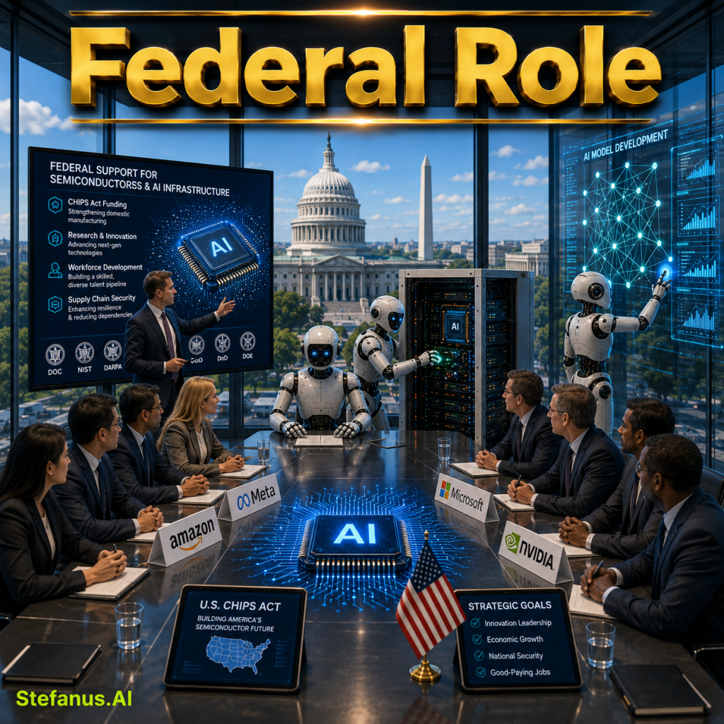
The United States federal government has reentered semiconductor policy because the market alone did not preserve domestic manufacturing leadership. The CHIPS and Science Act represents a recognition that advanced semiconductor capacity is too strategically important to leave entirely to offshore supply chains and quarterly corporate decisions. It is a reindustrialization instrument, a national-security policy, a workforce policy, and a geopolitical signal.
The Commerce Department states that CHIPS for America has allocated over $32 billion in proposed funding across 16 states and proposed additional billions for research and development.⁶ NIST describes CHIPS for America as the Department of Commerce program administering CHIPS incentives and semiconductor manufacturing support.²⁹
This is a major shift in American economic philosophy. For decades, the United States often prioritized design, software, finance, and consumption while allowing manufacturing to disperse globally. The AI era has exposed the weakness of that model. A country can lead in algorithms but remain vulnerable if it cannot manufacture the chips needed to run them.
5.1 What the CHIPS Act Gets Right
The CHIPS Act gets the central strategic premise right: semiconductor manufacturing is national infrastructure. It recognizes that the United States cannot rely entirely on Taiwan for leading-edge chips, cannot rely entirely on Asia for packaging and assembly, and cannot assume that global supply chains will remain stable under geopolitical stress.
The act also supports regional clusters. Semiconductor ecosystems do not emerge from single factories. They require supplier networks, universities, workforce pipelines, infrastructure, and local policy coordination. Arizona, Ohio, Texas, New York, and other states are now competing to become nodes in a revived semiconductor geography.
5.2 The Limitations of Federal Subsidy
But subsidy is not the same as execution. Semiconductor fabs require electricity, water, skilled labor, chemicals, tools, and long-term customer commitments. A federal grant can help build a fab, but it cannot instantly create a mature ecosystem.
The United States faces several limitations:
- Energy supply — AI data centers and semiconductor fabs both require large amounts of reliable electricity.
- Permitting delays — industrial projects often move slowly through environmental and local review.
- Workforce shortages — advanced fabs require technicians, engineers, and process experts.
- Supplier gaps — many critical upstream suppliers remain offshore.
- Cost differences — U.S. construction and operating costs can be higher than Asian alternatives.
- Customer trust — foundries must prove yield and reliability before customers commit advanced designs.
The United States can pass an industrial policy, but it must also rebuild industrial muscle memory. That is much harder.
5.3 Energy as the Constraint Behind the Constraint
The most underappreciated limitation is energy. Semiconductor fabs need reliable power, and AI data centers need even more. The IEA’s projection that data-center electricity consumption could reach 945 TWh by 2030 shows that the AI buildout will place sustained pressure on grids.⁴
This creates an uncomfortable reality: the CHIPS Act may support fabrication, but the AI economy also needs an energy act, a transmission act, a permitting act, a nuclear modernization strategy, and a data-center efficiency doctrine. Chips cannot be separated from electricity. Fabs cannot be separated from water. AI cannot be separated from land use.
This is why the first layer of Jensen Huang’s AI economy—energy—comes before chips. The sequence is correct. Semiconductor strategy without energy strategy is incomplete.
5.4 State Competition and the New Geography of AI Industry
States are becoming crucial actors. Arizona attracts TSMC. Texas attracts Tesla, SpaceX, Samsung, and potentially Terafab activity. Ohio is tied to Intel’s manufacturing ambitions. New York is positioning itself around semiconductor research and manufacturing. These state-level competitions matter because industrial policy is local in execution even when national in funding.
The federal government can provide incentives, but states provide permitting, infrastructure, workforce partnerships, tax policy, and land-use coordination. The future map of AI manufacturing may therefore be shaped as much by governors, utility commissions, and local development authorities as by federal agencies.
Section 6: What We Have Learned — Strategic Lessons from the AI Chip Race
The AI chip race teaches several strategic lessons that extend beyond semiconductors. It reveals how the digital economy has returned to physical infrastructure. It shows that software supremacy cannot survive without manufacturing capacity. It demonstrates that energy is not a background input but a central strategic constraint. It proves that geopolitics now runs through data centers, fabs, lithography tools, and memory supply chains. Most importantly, it shows that intelligence itself is becoming industrialized.
6.1 Lesson One: Compute Is Now Sovereign Infrastructure
The first lesson is that compute is no longer merely a commercial service. It is sovereign infrastructure. A nation’s AI capability depends on access to advanced chips, data centers, energy, and software ecosystems. Without compute, AI ambition remains theoretical.
This changes how governments think about technology. In the internet era, access to software platforms mattered. In the AI era, access to compute capacity matters just as much. The country or company that controls compute can influence which models are trained, which applications are affordable, which defense systems advance, and which scientific breakthroughs accelerate.
6.2 Lesson Two: Export Controls Are Economic Weapons
Export controls are now tools of economic warfare and strategic delay. Restricting access to advanced AI chips can slow a competitor’s model development, military AI systems, and scientific computing. But controls also have limits. They can incentivize smuggling, substitution, domestic development, and supply-chain workarounds.
The strategic challenge is to use controls precisely. Overbroad controls may harm domestic firms and accelerate rival self-sufficiency. Weak controls may allow adversaries to acquire strategic capabilities. The future of export control policy will require constant technical updating because chip architectures, performance thresholds, and model requirements evolve rapidly.
6.3 Lesson Three: The Bottleneck Moves
In the AI economy, bottlenecks migrate. At one moment, the bottleneck is GPUs. Then it becomes HBM. Then packaging. Then power. Then cooling. Then permitting. Then data. Then inference cost. A serious strategy must anticipate bottleneck migration rather than solving yesterday’s constraint.
This is why “Chip, Baby, Chip” must not become a narrow obsession with fabrication alone. The United States needs fabs, but also advanced packaging, memory supply, data-center power, grid modernization, cooling innovation, and skilled labor.
6.4 Lesson Four: Vertical Integration Is Returning
The AI era rewards vertical integration. Google designs TPUs and controls cloud infrastructure. Amazon designs Trainium and Inferentia for AWS economics. Meta builds MTIA for internal workloads. Tesla and SpaceX pursue Terafab logic. NVIDIA sells entire systems, not only chips.
This does not mean every company will own every layer. But it does mean that strategic firms want deeper control over their compute destiny. The companies that control more layers can optimize performance, reduce cost, secure supply, and move faster.
6.5 Lesson Five: Energy Efficiency Is National Security
Performance-per-watt is not merely an engineering preference. It is national security. If one country can produce the same AI capability using half the energy, it gains strategic advantage. If one hyperscaler can deliver inference at lower power cost, it gains margin and scale. If one military can deploy AI systems more efficiently at the edge, it gains operational advantage.
Vaclav Smil’s energy framing returns here. Energy is not separate from intelligence. It is the base currency.
6.6 Lesson Six: Orbital Compute Is No Longer Science Fiction
The most speculative but increasingly relevant lesson is that compute may move beyond Earth. Space-based data centers, orbital AI infrastructure, satellite-linked inference, and space-based solar concepts are emerging from the margins of imagination into early strategic discussion. Terafab’s reported connection to space-based data-center ambitions shows how far the logic of compute expansion can go.¹⁶
Orbital compute remains difficult. Radiation, launch cost, maintenance, heat dissipation, latency, and hardware replacement are serious barriers. But the fact that major technology actors are thinking in this direction reveals the scale of the AI infrastructure problem. If terrestrial grids become constrained, the imagination of compute will search for new geographies.
6.7 Lesson Seven: “More Chips” Is Not Enough
The final lesson is the most important. More chips are necessary, but not sufficient. The future requires:
- More efficient chips
- More domestic fabs
- More resilient supply chains
- More advanced packaging
- More power generation
- More transmission
- More water-conscious cooling
- More workforce training
- More allied coordination
- More export-control precision
- More architectural innovation
“Chip, Baby, Chip” must therefore mature from a slogan of acceleration into a doctrine of disciplined industrial strategy.

Conclusion: From Semiconductor Acceleration to Sovereign Compute Civilization
“Chip, Baby, Chip” begins as a slogan, but it ends as a diagnosis of the age. It captures the moment when artificial intelligence stopped being understood primarily as software and began to reveal itself as infrastructure. The AI revolution is not floating in the cloud. It is grounded in silicon, electricity, water, land, machinery, chemicals, labor, logistics, and geopolitics. The chatbot is only the front-end of a vast industrial machine.
The United States is right to recognize that AI leadership cannot survive without semiconductor strength. It is right to rebuild domestic manufacturing. It is right to support fabs through the CHIPS Act. It is right to work with allies. It is right to protect advanced compute from strategic misuse. It is right to encourage companies to build specialized chips, improve performance-per-watt, and reduce dependence on fragile chokepoints.
But the deeper lesson is that semiconductor acceleration must be disciplined by infrastructure realism. A nation cannot simply chant “Chip, Baby, Chip” and expect fabs, grids, lithography machines, HBM stacks, water systems, and skilled workers to appear. The physical world has timelines. Permits take time. Transmission takes time. Nuclear plants take time. Foundry credibility takes time. Yield learning takes time. Industrial ecosystems take time.
The danger of the AI era is that software ambition will outrun physical capacity. The opportunity of the AI era is that the United States can use this pressure to rebuild its industrial base, modernize its energy system, train a new generation of semiconductor workers, deepen alliances, and create a more resilient compute economy.
The final measure of success will not be who buys the most GPUs in one year, or who announces the largest fab, or who wins the loudest market cycle. The final measure will be who can build a durable compute civilization: one that converts energy into intelligence efficiently, manufactures chips securely, distributes compute responsibly, and protects democratic technological advantage without collapsing into wasteful acceleration.
“Chip, Baby, Chip” is therefore the opening cry of the AI hardware age. But the mature doctrine must be stronger:
Build the chips.
Power the chips.
Secure the chips.
Package the chips.
Cool the chips.
Govern the chips.
And above all, make every watt of intelligence count.
The future belongs not merely to the country that chips the fastest, but to the country that understands that chips are no longer components. They are the industrial grammar of artificial intelligence itself.

Footnotes
- Vaclav Smil, Energy and Civilization / MIT Press description of Smil’s work and energy framing. (MIT Press)
- Reuters, “Elon Musk lays out Terafab AI chip project plan”; Reuters, “SpaceX files plan for $55 billion Terafab chip facility in Texas.” (Reuters)
- International Energy Agency, “Key Questions on Energy and AI — Executive Summary,” April 14, 2026. (IEA)
- International Energy Agency, “Energy Demand from AI,” data-center electricity projection to 2030. (IEA)
- Chris Miller, Chip War quotation as excerpted in public quote listing. (Goodreads)
- U.S. Department of Commerce, “Semiconductor Industry / CHIPS for America.” (U.S. Department of Commerce)
- Reuters, “Nvidia restarting manufacturing of China AI chip variant,” March 17, 2026. (Reuters)
- Tom’s Hardware report on Jensen Huang comments at Milken Institute Global Conference, May 2026. (Tom’s Hardware)
- Reuters, “TSMC likely to book fourth straight quarter of record profit on insatiable AI demand,” April 2026. (Reuters)
- Reuters, “TSMC plans to open chip packaging plant in Arizona by 2029,” April 22, 2026. (Reuters)
- ASML, “EUV Lithography Systems.” (ASML)
- Georgetown CSET, “Tracing the Emergence of Extreme Ultraviolet Lithography.” (CSET)
- Reuters, “ASML unveils EUV light source advance that could yield 50% more chips by 2030,” February 2026. (Reuters)
- Intel, “Build with Leading-Edge Manufacturing Process Technologies.” (Intel)
- Intel Newsroom, “Intel Launches World’s First Systems Foundry Designed for the AI Era.” (Newsroom)
- Reuters, “SpaceX files plan for $55 billion Terafab chip facility in Texas,” May 2026. (Reuters)
- Reuters, “Elon Musk lays out Terafab AI chip project plan,” May 2026. (Reuters)
- Investing.com / Reuters factbox, “Elon Musk lays out Terafab AI chip project plan.” (Investing.com)
- Google Cloud, “Ironwood: The first Google TPU for the age of inference,” April 2025. (blog.google)
- Google, “Our eighth generation TPUs: two chips for the agentic era,” April 2026. (blog.google)
- Google Cloud, “Inside the Ironwood TPU codesigned AI stack,” November 2025. (Google Cloud)
- Amazon, “CPUs, GPUs, and accelerators: The chips powering AI,” May 2026. (Amazon News)
- AWS, “AWS Inferentia.” (Amazon Web Services, Inc.)
- AWS, “AWS Trainium.” (Amazon Web Services, Inc.)
- Meta AI, “Four MTIA Chips in Two Years.” (Meta AI)
- Meta, “Expanding Meta’s Custom Silicon to Power Our AI Workloads,” March 2026. (About Facebook)
- Reuters, “Meta unveils plans for batch of in-house AI chips,” March 2026. (Reuters)
- Reuters, “Nvidia to sell Meta millions of chips in multiyear deal,” February 2026. (Reuters)
- NIST, “CHIPS for America.” (nist.gov)